PN Junction:
When a manufacturer dopes a crystal so that one half of it is p-type and the other half is n-type,something new occurs. The area between p-type and n-type is called a pn junction.To form the
pn junction of semiconductor, an n-type region of the silicon crystal must be adjacent to or abuts a p-type region in the same crystal. The pn junction is characterized by the changing of doping from p type to n-type.
Depletion layer:
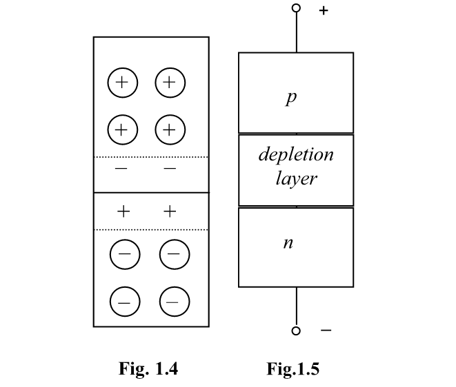
When the two substances are placed in contact, the free electrons of both come into equilibrium, both their number and the forces that bind them being unequal. Therefore, a transfer of electrons occurs, which continues until the charge accumulated is large enough to repel a further transfer of electrons.The accumulation of the charge at the interface acts as a barrier layer, called so due to its interfering with the passage of current.As shown in Fig. 1.4, the pn junction is the border where the p-type and the n-type regions meet. Each circled plus sign represents a pentavalent atom, and each minus sign is the free electron. Similarly, each circled minus sign is the trivalent atom and each plus sign is the hole. Each piece of a semiconductor is electrically neutral, i.e., the number of pluses and minuses is equal.
The pair of positive and negative ions of the junction is called a dipole.In the dipole, the ions are fixed in the crystal structure and they cannot move around like free electrons and holes. Thus, the region near the junction is emptied of carriers. This charge-empty region is called the depletion layer also because it is depleted of free electrons and holes.The ions in the depletion layer produce a voltage across the depletion layer known as the barrier potential. This voltage is built into the pn junction because it is the difference of potentials between the ions on both sides of the junction. At room temperature, this barrier potential is equal approximately to 0,7 V for a silicon dipole.

No comments:
Post a Comment