Showing posts with label Basic Electronics. Show all posts

Sunday, 10 May 2015

DEFINE RESISTORS,CAPACITORS & INDUCTORS


The three basic elements used in electronic circuits are the resistor, capacitor, and inductor. They each play an important role in how an electronic circuit behaves. They also have their own standard symbols and units of measurement. 

Resistors:

A resistor represents a given amount of resistance in a circuit. Resistance is a measure of how the flow of electric current is opposed or "resisted." It is defined by Ohm's law which says the resistance equals the voltage divided by the current. 

Resistance = voltage/current 
or 
R = V/I


Resistance is measured in Ohms. The Ohm is often represented by the omega symbol: Ω. 

The symbol for resistance is a zigzag line as shown below. The letter "R" is used in equations. 

Capacitors:

A capacitor represents the amount of capacitance in a circuit. The capacitance is the ability of a component to store an electrical charge. You can think of it as the "capacity" to store a charge. The capacitance is defined by the equation.

C = q/V 
where q is the charge in coulombs and V is the voltage.


In a DC circuit, a capacitor becomes an open circuit blocking any DC current from passing the capacitor. Only AC current will pass through a capacitor. 

Capacitance is measured in Farads. 

The symbol for capacitance is two parallel lines. Sometimes one of the lines is curved as shown below. The letter "C" is used in equations. 

Inductors:

An inductor represents the amount of inductance in a circuit. The inductance is the ability of a component to generate electromotive force due to a change in the flow of current. A simple inductor is made by looping a wire into a coil. Inductors are used in electronic circuits to reduce or oppose the change in electric current. 

In a DC circuit, an inductor looks like a wire. It has no affect when the current is constant. Inductance only has an effect when the current is changing as in an AC circuit. 

Inductance is measured in Henry. 

The symbol for inductance is a series of coils as shown below. The letter "L" is used in equations. 
Read more ...

Saturday, 9 May 2015

DC AMPLIFIERS

Fundamental Specifications:

The fundamental specifications of dc amplifiers are as follows:
  - input/output signal range,
  - offset and offset drift,
  - single or balanced supply,
  - input bias current,
  - open loop gain,
  - integral linearity,
  - voltage and current noise.

DC Amplifier:


As shown in the below diagram, the direct coupled amplifier (DC) is consist of two transistors Q1 and Q2 , a voltage divider base bias resistor network (R1, R2) which is provided on the transistor Q1 base two collector resistors Rc1and Rc2, the transistor Q2 is self biased, we also use tow emitter by pass resistors RE1and RE2. The direct-coupled amplifier is operated with out the using of frequency sensitive component like capacitor, inductor and Transformer etc. The direct coupled amplifier amplify the A.C signal with frequency as low a fraction of Hertz (Hz).

First of all when we applied a +ve half cycle at the I/P of Q1 transistor, which is already biased through the divider bias network. The +ve half cycle forwarded bias the transistor Q1 which start the conduction and give an inverted and amplified O/P  at the collector . As we know that,

VCE= Vcc - IcRc


This amplified -ve signed is provided to the base of Q2 transistor, which is self-bias (because they are connected in cascade condition). The base  of Q2 transistor  is a reversed  and did not  conduct,  the O/P of transistor Q2 is amplified  signal  (inverting to I/P of Q2) when the Q2 did not  conduct and the voltage  drop across collector  emitter  will be zero, therefore  the VCC is equal  to IcRc.

The O/P equal  to the voltage  drop  across the collector  resistors.

Applications:


-Pulse amplifier.
-Differential Amplifier.
-Regulator circuits of electronic power supply.
-Computer circuitry.
-Jet engine control.
-Electronic instruments.
Read more ...

AC AMPLIFIERS

AC Amplifiers:

Altering of a voltage or current signal size as it is passed through a system is called an amplitude control.An amplifier is a circuit for the amplitude control provision. Except for early relatively inefficient electromechanical amplifiers, electronic amplifier development started with the invention of the vacuum tube.Classes of amplifiers.Amplifiers are classified according to the polarity and properties of the output current or voltage. Their characteristics cover one, two, or four quadrants on the axes plane. The ac amplifiers and dc amplifiers are distinguished. The fundamental specifications of ac amplifiers are listed on their data sheets; usually they include.
- small-signal and large-signal bandwidths,
- voltage and current band noise,
- harmonic distortion level,
- input and output impedances,
- current and voltage gains.
It is common knowledge that amplifiers are divided into some general classes - A, B, C, etc., depending on the type of service in which they are to be used.


A class A amplifier is one which operates in the transistor’s active region so that the output wave shapes of current are practically the same as those of the existing input signal at all times. Fig. 2.9 illustrates the typical transfer graphs of the collector current versus the base current. For the class A amplifier (Fig. 2.9,a), if the input signal is sinusoidal, the output signal is also sinusoidal. Consequently, the low clipping is the main advantage of this mode of operation. For this reason, the amplifiers of such kind are known as linear amplifiers.Low efficiency (30 to 45%) is the main drawback of the class A amplifier. 
For this reason, it is commonly used in low-power applications and preamplifiers.A class B amplifier operates with a negative bias approximately equal to cutoff. Its base voltage is more negative than in the class A amplifier. Therefore, the output current is almost zero when the alternating input signal is removed or negative (Fig. 2.9,b). With a sinusoidal signal applied, the output consists of a series of half-sine waves. A bottom part of this half-wave is distorted, and the border of this distortion is called a cutoff zone.The amplifiers of such kind are known as pulse amplifiers with high clipping. Efficiency of the class B amplifier is higher (45 to 70%) than in the class A amplifier. For this reason, they are used as the balanced output stages. More often, the intermediate class AB is selected, the clipping of which is much less.
A class C amplifier operates with a negative bias essentially less than cutoff. It passes the current during the part of the positive alternation only. The output current has narrow width and its shape distortion is maximal (Fig. 2.9,c). Its high efficiency (70 to 90%) is the primary considerations at radio frequencies higher than 20 kHz. The class C amplifiers are preferable in power amplifiers with resonance load, for example, transmitters.A class D amplifier uses transistors as switches where the only modes are switch on and switch off. It is used in different switching circuits.
Read more ...

Thursday, 7 May 2015

WHAT IS THYRISTOR ?


Thyristors:

Thyristor name is derived from the Greek “thyra” and means “door”, that is allowing something to pass through. The main group of thyristors is composed by SCR, and others are the special-purpose devices.


Structure:

silicon-controlled rectifier (SCR) consists of a four-layer silicon wafer with three pn junctions.
It has four doped regions, the anode (A), the cathode (C), and the gate (G). The gate is the control lead. The SCR is triggered into conduction by applying a gate-cathode voltage, which causes a specific level of gate current. The device is returned to its non-conducting state by either anode current interruption or forced commutation.When the SCR is turned off, it stays in a non-conducting state until it receives another trigger. Therefore, the SCR can be termed as one operation thyristor-or 
rectifier thyristor.The structure, biasing circuit, and possible symbols of thyristors are shown in Fig. 1.48. First of them displays the anode-side SCR with an  n-gate lead, the second is the cathode-side thyristor with a  p-gate lead, and the last is the most common device. High-voltage high-power thyristors sometimes also have a fourth terminal, called an auxiliary cathode,used for connection to the triggering circuit. This prevents the main circuit from interfering with the gate circuit. 
Thyristors are commonly used in adjustable ac rectifier circuits, especially in power units up to 100 MVA. Their frequency capabilities are not high, in fact lower than 10 kHz. 

Output characteristics:

 Fig. 1.49 illustrates the output curves and idealized output characteristics of a thyristor. The device has two operating regions: non-conducting and conducting. The current–voltage output characteristics for different gate currents show the forward bias. The output characteristic of a 
thyristor in the reverse bias is very similar to the same curve of the diode with a small leakage current.Using the same arguments as for diodes, the thyristor can be represented by the idealized characteristic in analyzing the circuit-desired topologies.

When it is non-conducting, the thyristor operates on the lower line in the forward blocking state (off 
state) with a small leakage current. The thyristor is in off state until no current flows in the gate. The 
short firing pulse below the breakover voltage from the gate driver  triggers the thyristor. This current pulse may be of triangle, rectangle, saw-tooth, or trapezoidal shape.When a thyristor is supplied by ac, the moment of a thyristor firing should be adjusted by shifting the control pulse relative to the starting point of the positive alternation of anode voltage. This delay is called a 
control angle or firing angle.In dc circuits, the use of thyristors is complicated due to their turning on/off.After the pulse of the gate driver is given, the thyristor breaks over and switches along the dashed line to the conducting region. The dashed line in this graph indicates an unstable or temporary condition.The device can have current and voltage values on this line only briefly as it switches between the two stable operating regions. Once turned to the on state and the current higher than the 
holding current,the thyristor remains in this state after the end of the gate pulse.When the thyristor is conducting, it is operating on the upper line. The current (up to thousands of amperes) flows from the anode to the cathode and a small voltage drop (1 to 2 V) exists between them. If the current tries to decrease to less than the holding border, the device switches back to the non-conducting region.
Turning off by gate pulse is impossible. Thyristor turns off when the anode current drops under the 
value of the holding current.


Input characteristics:

Fig. 1.50 illustrates the input characteristics of the thyristor. The curves show the relation between the gate current and the gate voltage. This relation has a broad coherence area with a width that depends on the temperature and design properties of the device.

The gate current has an effect upon the form of the characteristic. The value of the breakover voltage is the function of the gate current. The more is the gate current the lower is the voltage level required to switch on the thyristor. Maximum breakover voltage of a thyristor reaches up to thousands of volts. If the applied voltage exceeds the breakover level, SCR triggers without the gate pulse. This prohibited mode should be avoided.
Read more ...

DEFINE TRANSISTORS


Transistors:

A transistor regulates current or voltage flow and acts as a switch or gate for electronic signals. A transistor consists of three layers of a semiconductor material, each capable of carrying a current. A semiconductor is a material such as germanium and silicon that conducts electricity in a "semi-enthusiastic" way. It's somewhere between a real conductor such as copper and an insulator (like the plastic wrapped around wires).

The semiconductor material is given special properties by a chemical process called doping. The doping results in a material that either adds extra electrons to the material (which is then called N-type for the extra negative charge carriers) or creates "holes" in the material's crystal structure (which is then called P-type because it results in more positive charge carriers). The transistor's three-layer structure contains an N-type semiconductor layer sandwiched between P-type layers (a PNP configuration) or a P-type layer between N-type layers (an NPN configuration).

A small change in the current or voltage at the inner semiconductor layer (which acts as the control electrode) produces a large, rapid change in the current passing through the entire component. The component can thus act as a switch, opening and closing an electronic gate many times per second. Today's computers use circuitry made with complementary metal oxide semiconductor (CMOS) technology. CMOS uses two complementary transistors per gate (one with N-type material; the other with P-type material). When one transistor is maintaining a logic state, it requires almost no power.

Transistors are the basic elements in integrated circuits (ICs), which consist of very large numbers of transistors interconnected with circuitry and baked into a single silicon microchip or chip.

Common Features of Transistors:

The word “transistor” was coined to describe the operation of a “transfer resistor”. First, a point contact transistor was produced. It included two diodes placed very closely together such that the current in either diode had an important effect upon the current in the other diode. By the proper biasing the diodes, it was possible to obtain power amplification of electric signals between the diode common layer, which lead was called a base,and other layers. One of the leads of this device was designated as an emitter, the corresponding diode was biased in the forward direction, the other was   
a collector and its diode was biased in the reverse direction. Power amplification was obtained by virtue of the fact that the few variations in the base current caused a large variation in the emitter-collector current. The point-contact transistor had certain drawbacks:

- High sensitivity to temperature, either ambient or self-generated;

- Production problems, i.e., a difficulty to reproduce the same electrical qualities in close tolerance for mass production.

-Low amplification, especially at high frequencies.

Intensive research has been done to diminish or remove these drawbacks. As a result, developers have produced semiconductor materials that are not so sensitive to temperature, inexpensive, operate at high frequencies, have low power dissipation, and internal noise of the transistor. A device, which is more stable both mechanically and electrically, has been constructed by forming junctions rather than point contacts. General classes of transistors that are used in electronics today are as follows:


- Bipolar junction transistors (BJT).
- Junction field-effect transistors (JFET).
- Metal-oxide semiconductor field-effect transistors (MOSFET) up to some kilowatts, hundreds amperes, and tenths gigahertz.
- Insulated-gate bipolar transistors (IGBT) up to thousands of kilowatts, some kiloamperes, 
and hundreds kilohertz.

More powerful devices have been built on the thyristors though IGBTs have the potential to  
replace them.

Read more ...

Wednesday, 6 May 2015

DEFINE ZENER DIODE


Zener diode:

 A Zener diode sometimes called breakdown diode or stabilitrone,is designed to operate in the reverse breakdown, or Zener, region, beyond the peak inverse voltage rating of normal diodes. This reverse breakdown voltage is called the Zener or, reference voltage, which can range between –2,4 V and –200 V (Fig. 1.12). The Zener effect causes a “soft” breakdown whereas the avalanche effect causes a 
sharper turnover. Both effects are used in the Zener diode. The manufacturer predetermines the Zener and avalanche voltages. 


A significant parameter of the Zener diode is the temperature coefficient that is the breakdown voltage deviation during the temperature rise or fall. The temperature coefficient of the Zener diode changes from negative to positive near –6 V. Because of this, by selecting the current value the designer may minimize the instability of the device. In all types of devices, the output levels are affected by variations in the load. Lower percentage values, approaching 0%, indicate better regulation. The Zener diode is the backbone of voltage regulators, circuits that hold the load voltage constant despite the large changes in line voltage and load resistance. When used as a voltage regulator, the Zener diode is reverse biased so that it will operate in the breakdown region with highly stable Zener voltage. In this region, changes in current through the diode have no effect on the voltage across it. The Zener diode establishes a constant voltage across the load within a range of output voltages and currents. Out of this range, the voltage drop remains constant and the current flow through the diode will vary to compensate the changes in load resistance.A power Zener diode is called an avalanche diode.It can withstand kilovolts voltages and currents of some thousands of amperes.
Read more ...

POWER DIODE AND ITS CHARACTERISTICS


Power Diode:

A power diode is more complicated in structure and operational characteristics than the small-signal 
diode. It is a two-terminal semiconductor device with a relatively large single pn junction, which consists of a two-layer silicon wafer attached to a substantial copper base. The base acts as a heat sink, a support for the enclosure and one of electrical leads of the device. The extra complexity arises from the modifications made to the small-signal device to be adapted for power applications. These features are common for all types of power semiconductor devices.

Characteristics:

In a diode, large currents cause a significant voltage drop. Instead of the conventional exponential output relationship for small-signal diodes, the forward bias characteristic of the power diode is approximately linear. This means the voltage drop is proportional both to the current and to ohmic resistance. The maximum current in the forward bias is a function of the area of the pn junction. 
Today, the rated currents of power diodes are thousands of amperes and the area of the pn junction may be tens of square centimeters. The structure and the method of biasing of a power diode are displayed in Fig. 1.9. The anode is connected to the   layer and the cathode to the p substrate layer n. In the case of power diode, an additional n layer exists between these two layers. This layer termed as a drift region can be quite wide for the diode. The wide lightly doped region adds significant ohmic resistance to the forward-biased diode and causes larger power dissipation in the diode when it is conducting current.

Forward biasing:

 Most power is dissipated in a diode in the forward-biased on-state operation.For small-signal diodes, power dissipation is approximately proportional to the forward current of the diode. For power diodes, this formula is true only with small currents. For large currents, the effect of ohmic resistance must be added. In a high frequency switching operation,significant switching losses will appear when the diode goes from the off-state to the on-state, or vice versa. Real operation currents and voltages of power diodes are essentially restricted due to power losses and the thermal effect of power dissipation. Therefore, in power devices cooling is very important.

Reverse biasing:


In the case of reverse-biased voltage, only the small leakage current flows through the diode. This current is independent of the reverse voltage until the breakdown voltage is reached. After that, the diode voltage remains essentially constant while the current increases dramatically. Only the resistance of the external circuit limits the maximum value of current. Large current at the breakdown voltage operation leads to excessive power dissipation that should quickly destroy the diode. Therefore, the breakdown operation of the diode must be avoided.To obtain a higher value of breakdown voltage, the three measures could be taken. First, to grow the breakdown voltage, lightly doped junctions are required because the breakdown voltage is inversely proportional to the doping density. Second, the drift layer of high voltage diodes must be sufficiently wide. It is possible to have a shorter drift region (at the same breakdown voltage) if the depletion layer is elongated. In this case, the diode is called   a punch-through diode.The third way to obtain higher breakdown voltage is the boundary control of the depletion layer. All of these technological measures will result in the more complex design of power diodes.

Switching:

 For power devices, switching process is the most common operation mode. A power diode requires a finite time interval to switch over from the off state to the on state and backwards. During there transitions, current and voltage in a circuit vary in a wide range. This process is accompanied with energy conversion in the circuit components. A power circuit contains many components that can 
store energy (reactors, capacitors, electric motors, etc.). Their energy level cannot vary instantaneously because the power used is restricted. Therefore, switching properties of power devices are analyzed at a given rate of current change, as shown transients in Fig. 1.10.


The most essential data of power switching are the forward voltage overshoot U(F max) when a diode turns on and the reverse current peak value I(R max) when a diode turns off.

Summary:

Power diode is adapted for switching power applications. In addition to bulk resistance, it has high ohmic resistance. To withstand the essential losses that appear when the diode goes from the off state to the on state and backward, cooling is very important. To obtain a higher value of breakdown voltage, some measures are usually taken, such as lightly doped junctions, sufficiently wide drift layer, and the boundary control of the depletion layer. These measures result in a more complex design of power diodes but shorten the reverse recovery time and increase their lifetime.

Special-Purpose Diodes:

Rectifier diodes are used in the circuits of 50 Hz to 50 kHz frequencies. They are never intentionally 
operated in the breakdown region because this may damage them. They cannot operate properly under abnormal conditions and high frequency. Devices of other types have been developed for such kind of operations.
Read more ...

DEFINE BIASING ?

Biasing:

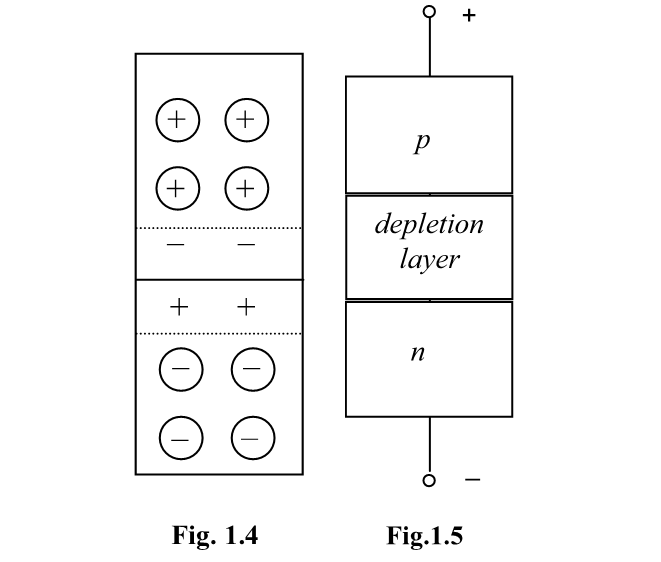
 Fig. 1.5 shows a dc source (battery) across a pn junction. The negative source terminal is connected to the n-type material, and the positive terminal is connected to the p-type material. Applying an external voltage to overcome the barrier potential is called the forward bias.If the applied voltage is 
greater than the barrier potential, the current flows easily across the junction. After leaving the negative source terminal, an electron enters the lower end of the crystal. It travels through the   region as a free n electron. At the junction, it recombines with a hole, becomes a valence electron, and travels through the p region. After leaving the upper end of the crystal, it flows into the positive source terminal.Application of an external voltage across a dipole to aid the barrier potential by turning the dc source around is called the reverse bias.The negative source terminal attracts the holesand the positive terminal attracts the free electrons. Because of this, holes and free electrons flow away from the junction. Therefore,the depletion layer is widened. The greater the reverse bias, the wider the depletion layer will be. Therefore, the current will be almost zero.


Forward biasing:

When the positive terminal of the battery is connected to the p-type material and the negative terminal of the battery is connected to the n-type material, such a connection is called forward bias.

Above figure shows the p-n junction diode in forward bias condition. The p region is connected to the positive terminal and n region is connected to the negative terminal of the DC voltage source. A resistor is also connected in series with the diode to make sure the current in the circuit does not rise above the maximum limit and damage the diode. When the diode is forward biased, the electric field in the depletion region and the external electric field due the DC voltage source are in opposite direction (This is shown in the above figure). This reduces the effective/net electric field in the depletion region. Recall that in the previous section on p-n junction diode, we had discussed that the flow of electrons and holes ceased due to the electric field. Since the net electric field is now reduced due to forward bias, electrons and holes now crosses the junction and constitutes a current. The direction of current is from p-region to n-region.
                                                                            The flow of current can be explained as follows. The electrons and holes crosses the p-n junction as a result of reduced electric field in the depletion region. Electrons from the n-region crosses the junction and enters the p-region.Since the positive terminal of the battery is connected to the p-region, the electrons experiences an attractive force and moves to the positive terminal of the battery. Same discussion can also be applied to holes. Thus we can conclude that current flow takes place when the diode is forward biased.
Now we shall see the effect of applying forward bias to the diode. The topics we shall discuss are as follows:

Effect on depletion region due to forward bias
Effect of barrier potential during forward bias

Effect on depletion region due to forward bias:

When the diode is connected in forward bias, the electric field due to external voltage source and the electric field due to depletion region are in the opposite direction. This reduces the net electric field in the junction and the electrons can now pass from n-region to the p-region. As more electrons now flows into the depletion region, the number of positive ions is reduced. Same discussion can also be applied to holes. With the reduction in net electric field, the holes can now flow into the n-region. As the holes pass through the depletion region, the number of negative ions also decreases. Hence the the width of depletion region decreases due to reduction in the number of positive and negative ions. This is shown graphically in the figure below.


Effect of barrier potential during forward bias:

Before preceding with this discussion, let us have a quick revision of what is  called as barrier potential (the concept is explained in detail here). When p-type and n-type materials are joined together, the electrons from n-type material starts to move towards p-type material and forms negative ions. Similarly the holes from the p-type material starts to move towards n-type material and forms positive ions. This separation of  positive and negative ions creates an electric field. When the electric field becomes sufficiently strong, it prevents further movement of electrons and holes. The potential resulting from such electric field act as barrier for further movement of electrons and holes. This potential is called barrier potential.
                                                               Now we come to the actual discussion- what is the effect of barrier potential when the diode is forward biased? When no bias is applied, the electrons cannot gain sufficient energy to overcome the potential barrier and move to the p-region. With the diode is forward biased, the electrons get enough energy from the voltage source to overcome the potential barrier and cross the junction. Similarly the holes get sufficient energy to overcome the barrier and cross the junction. The amount of energy required by the electrons to cross the junction is equal to the barrier potential (0.3 V for Ge and 0.7 V for Si). This simply means that when the diode is forward biased, the voltage drop across the diode is approximately 0.7 V (for Si). Actually, the amount of voltage drop is little above 0.7 V due to internal resistance of the material and contact resistance of the conducting material used to form the legs of diode.

Reverse Biasing:

When the positive terminal of the battery is connected to n-type material and the negative terminal of the  battery is connected to p-type material, such a connection is called reverse bias.


Above figure shows the diode connected in reverse bias. You can clearly see that the negative terminal of the battery is connected to p-type material and the positive terminal of the battery is connected to n-type material. A resistor is also connected in series with the diode, although resistor is not required when the diode is reverse biased. When the diode is reverse biased, the electric field due to the battery and the electric field of the depletion region are in the same direction. This makes the electric field even stronger than that before reverse bias was applied. The electrons from the n-type material (majority carriers) now faces a stronger electric field and it becomes even more difficult for them to move towards the p-type material. Same discussion also applies to holes. The holes from the p-type material (majority carriers) now faces a stronger electric field and it becomes even more difficult to move from p-type to n-type material.Hence we conclude that there is no flow of current due to majority carriers when the diode is reverse biased.

We shall discuss following important points with regards to the reverse biased p-n junction.

Effect of reverse bias on the width of depletion region.
Reverse saturation current.
Reverse breakdown volatge.

Effect of reverse bias on the width of depletion region:

Let us discuss how the width of depletion region changes when the reverse bias is applied. When the positive terminal of the battery is connected to the n-type semiconductor, the electrons from the n-type semiconductor are quickly drawn towards the positive terminal. (Refer the above figure). This reduces the number of majority carriers in n-type semiconductor. As the number of electrons reduces, additional positive ions are created. Similarly the holes from the p-type semiconductor are attracted towards the negative terminal of the battery. This reduces the number of holes in the p-type semiconductor and hence additional negative ions are created in the p-type material. Hence we conclude that as the number of positive and negative ions increases, the width of the depletion region increases. This is shown graphically in the figure below.

Reverse saturation current"


We saw in the earlier section that there is no flow of current due to majority carriers when the diode is reverse biased. However there is a very little flow of current (in nano ampere range for silicon diode) due to minority carriers that are produced in the crystal due to thermal energy. When the diode is reverse biased, the electrons from the p-type semiconductor are pushed towards the p-n junction by the negative terminal of the battery. Similarly the holes from the n-type semiconductor are pushed towards the junction by the positive terminal of the battery. This movement of electrons and holes constitutes a current called reverse saturation current.  The term saturation refers to the fact that it reaches its maximum value very quickly and does not change significantly with increase in reverse bias potential.

Reverse breakdown voltage:


The magnitude of reverse current is of the order of nano-amperes for silicon devices. This current does not change significantly with the applied reverse bias potential. However, when the reverse bias is increased beyond a certain limit, the reverse current increases drastically. The voltage beyond which the reverse current increases drastically is called reverse breakdown voltage. The diode is said to undergo breakdown when the voltage is increased above breakdown voltage. Two mechanisms for diode breakdown are recognized- Avalanche breakdown and Zener breakdown. Both these mechanisms are discussed in detail in the section on avalanche and zener breakdown.


Read more ...

WHAT IS PN JUNCTION ?

PN Junction:

When a manufacturer dopes a crystal so that one half of it is p-type and the other half is n-type, 
something new occurs. The area between  p-type and  n-type is called  a pn junction.To form the 
pn junction of semiconductor, an  n-type region of the silicon crystal must be adjacent to or abuts a p-type region in the same crystal. The pn junction is characterized by the changing of doping from  p type to n-type. 

Depletion layer:

When the two substances are placed in contact, the free electrons of both come into equilibrium, both their number and the forces that bind them being unequal. Therefore, a transfer of electrons occurs, which continues until the charge accumulated is large enough to repel a further transfer of electrons.The accumulation of the charge at the interface acts as a barrier layer, called so due to its interfering with the passage of current.As shown in Fig. 1.4, the pn junction is the border where the  p-type and the  n-type regions meet. Each circled plus sign represents a pentavalent atom, and each minus sign is the free electron. Similarly, each circled minus sign is the trivalent atom and each plus sign is the hole. Each piece of a semiconductor is electrically neutral, i.e., the number of pluses and minuses is equal.


The pair of positive and negative ions of the junction is called a dipole.In the dipole, the ions are fixed in the crystal structure and they cannot move around like free electrons and holes. Thus, the region near the junction is emptied of carriers. This charge-empty region is called the depletion layer also because it is depleted of free electrons and holes.The ions in the depletion layer produce a voltage across the depletion layer known as the barrier potential. This voltage is built into the pn junction because it is the difference of potentials between the ions on both sides of the junction. At room temperature, this barrier potential is equal approximately to 0,7 V for a silicon dipole.
Read more ...

DEFINE DOPING

Doping:  

One way  to  raise  conductivity  is  by doping.This means adding impurity atoms to a  pure tetravalent crystal (intrinsic crystal). A doped material is called an extrinsic semiconductor.Impurity 
atoms added to the semiconductor change the thermal equilibrium density of electrons and holes. In 
the case of silicon, the appropriate impurities are elements from the 5  and 3  columns of the periodic table, e.g. such as phosphorus and boron. By doping, two types of semiconductors may be produced.First of them are n-type semiconductors with a pentavalent (phosphorus) impurity where the   stands n for negative (Fig. 1.3) because their conduction is due to a transfer of excess electrons.A pentavalent atom, the one that has five valence electrons is called a donor.Each donor produces one free electron in a silicon crystal. In an  -type semiconductor, the free electrons are the n majority carriers, while the holes are the minority carriers because the free electrons outnumber the holes.
The addition of impurities to a semiconductor to achieve a desired characteristic, as in producing an n-type or p-type material. Also known as semiconductor doping.

Basic conditions that are required for the doping process are given below:

1.The atom which is to be doped in the crystal must be placed at the position same as that of the position of the semiconductor atom.

2.There should be no distortion in the crystal after the insertion of the dopants.

3.The size of the dopants should be exactly same as that of the size of the atom of the crystal.

4.In a crystal the percentage of doping should not be more than one percent.

Some basic doping techniques of doping are shown below:

1.First we have to heat up the semiconductor crystal. The heating must be at the place where the dopants are present in the atmosphere. After heating the diffusion of the dopants will take place in the lattice site of the crystal.

2.In the second method of doping, the semiconductor is bombarded with the ions of the semiconductor itself. Then the dopants are embedded.
Read more ...

TYPES OF SEMI-CONDUCTOR DEVICES


Intrinsic Semiconductors.

 The density of free carriers defines the conductivity of semiconductors as an intermediate between that of insulators and conductors. As mentioned above, the density of free carriers of metals and insulators is approximately constant. This is exact opposite for semiconductors, where the free carrier density can be changed by many orders. This feature of semiconductors, their ability to manipulate by free carrier density, is very significant in many electronic applications. The reason of this phenomenon is next.Conduction of semiconductors takes place by electrons just as in metals, but,contrary to the behavior of metals, a substance of this kind exhibits a growing of resistance as the temperature falls. The resistance of the semiconductor material is called a bulk resistance.Since the resistance decreases as the temperature increases, it is a negative resistance, and semiconductor is called a negative temperature coefficient device.Such a substance is referred to as a semiconductor because at the absolute zero of temperature, it would be an insulator and at a very high temperature, it is a conductor. At room temperature, a pure silicon crystal has only a few thermally produced free electrons. Any temperature rise will result in thermal motion of atoms. This process is called thermal ionization.The higher the ambient temperature, the stronger is the mechanical vibration of atoms and the lattice. These vibrations can dislodge an electron from the valence orbit. For example, if the temperature changes some ten degrees centigrade, the electrical resistance of pure germanium changes several hundred times.The materials the conductivity of which is found to increase very strongly with increasing temperature are called intrinsic semiconductors.
                                                                                                                  The name “intrinsic” implies that the property is a characteristic of pure material that has nothing but silicon or germanium atoms.They are not only characterized by the resistive factor but also by the great influence that various factors, such as heat and light, have upon conductivity.

Extrinsic Semiconductors:

Those semiconductors in which some impurity atoms are embedded are known as extrinsic semiconductors.

Extrinsic semi conductors are basically of two types:
1. P-type semi conductors
2. N-type semi conductors

N-type Semi conductors:
 Let’s take an example of the silicon crystal to understand the concept of N-type semi conductor. We have studied the electronic configuration of the silicon atom. It has four electrons in its outermost shell. In N-type semi conductors, the silicon atoms are replaced with the pentavalent atoms like phosphorous, bismuth, antimony etc. So, as a result the four of the electrons of the pentavalent atoms will form the covalent bonds with the silicon atoms and the one electron will revolve around the nucleus of the impurity atoms with less binding energy. These electrons are almost free to move. In other words we can say that these electrons are donated by the impure atoms. So, these are also known as donor atoms. So, the conduction inside the conductor will take place with the help of the negatively charged electrons. Electrons are negatively charged. Due to this negative charge these semiconductors are known as N-type semiconductors.

Each donor atom has denoted an electron from its valence shell. So, as a result due to loss of the negative charge these atoms will become positively charged. The single valence electron revolves around the nucleus of the impure atom. Some experiments were performed. It was found that .01eV and .05eV energy is required to make the electron free from the nuclear forces.

When the semi conductors are placed at room temperature then the covalent bond breakage will take place. So, more free electrons will be generated. As a result, same no of holes generation will take place. But as compared to the free electrons the no of holes are comparatively less due to the presence of donor electrons.

We can say that major conduction of n-type semi conductors is due to electrons. So, electrons are known as majority carriers and the holes are known as the minority carriers.


N-type Semi conductors:

P-type semi conductors: In a p-type semi conductor doping is done with trivalent atoms .Trivalent atoms are those which have three valence electrons in their valence shell. Some examples of trivalent atoms are Aluminum, boron etc. So, the three valence electrons of the doped impure atoms will form the covalent bonds between silicon atoms. But silicon atoms have four electrons in its valence shell. So, one covalent bond will be improper. So, one more electron is needed for the proper covalent bonding. This need of one electron is fulfilled from any of the bond between two silicon atoms. So, the bond between the silicon and indium atom will be completed. After bond formation the indium will get ionized. As we know that ions are negatively charged. So, indium will also get negative charge. A hole was created when the electron come from silicon-silicon bond to complete the bond between indium and silicon. Now, an electron will move from any one of the covalent bond to fill the empty hole. This will result in a new holes formation. So, in p-type semi conductor the holes movement results in the formation of the current. Holes are positively charged. Hence these conductors are known as p-type semiconductors or acceptor type semi conductors.


When these conductors are placed at room temperature then the covalent bond breakage will take place. In this type of semi conductors the electrons are very less as compared to the holes. So, in p-type semi conductors holes are the majority carriers and electrons are the minority carriers.

Read more ...

SEMI-CONDUCTOR DEVICES

Semiconductor Devices:

To understand how electronic devices operate, one has first to learn about the atomic structure  
of matter.

Structure of matter:

The matter consists of atoms, which contain electrons and  a nucleus with protons and neutrons in a particularly intimate association. The electron has a negative charge. The proton has a positive charge equal to the negative charge carried by the electron. The neutron, as its name implies,has no charge; it is electrically neutral. Each element possesses a certain number of protons and an equal number of electrons to keep the atom electrically neutral. Each element is characterized by its number of electrons, or as it is called, its atomic number.The electrons are spread out in space around the nucleus in shells, which have been compared to the orbits of the planets round the sun. The electrons can be often stripped off the atom rather easily, leaving it positively charged, naturally, but it is much more difficult to break up the nucleus.

Current:

Electric current flows in a material being a result of the interaction of charged pieces called carriers
. A review of the mechanism for conducting electricity through various kinds of matter shows that in electrolytes and in gases, conduction occurs through the motion of ions.In metallic conductors, conduction takes place via the motion of electrons, and there is no conduction in insulators,but only a slight displacement of the charges within the atoms themselves. The number of free carriers in different materials varies in an extremely wide range. In metals, the density of free electrons is in order of 10^23 1/cm.In insulators, the free electron density is less than 10^3 1/cm . For this reason, the electrical conductivity of 33 various materials is very different, more than 10^6  S/cm for metals and less than 10^15 S/cm for insulators.

Energy levels:

The negatively charged electrons possess energy in discrete amounts, and therefore they 
are placed only in certain energy levels without gaps between them. In the normal state, the electrons 
tend to fill the lowest energy levels, leaving only the highest energy level unfilled. Electrons in this outer shell are loosely bound to the nucleus and can be freed or tied to neighboring atoms. In solids,atoms are situated very closely to each other. Neighboring atoms can derange their energy levels and combine to form energy bonds. Only the outer orbit is of interest to understanding the conductivity properties in a solid, also called the valence bond where electrons can move and participate in an electric current. Between the valence and other bonds, there is a forbidden gap, which the electrons can cross but where they cannot remain.

Conductivity:

The key to electrical conductivity of chemical elements is the number of electrons in the valence orbit. Insulators have up to eight valence electrons. Some of the atoms of the conductor have only one valence electron in their outer orbit. Since this single electron can be easily dislodged from its atom, it is called a free electron or a conduction-bond electron because it travels in a large orbit,equivalent to a high energy level. The slightest voltage causes free electrons to flow from one atom to another. The density of free carriers of metals and insulators is approximately constant and cannot be changed in a marked range. The electrical resistance of a metal changes slightly with temperature. The variation of resistance with temperature is accounted for as follows. In a metal only very few electrons are free to move upon application of a potential difference. The temperature of the conductor being lowered, the thermal vibration of its atoms’ lattice is decreased. As a result, the atoms interfere less with the motion of electrons, and consequently, the resistance is lowered. Such kind of resistance is known as an ohmic resistance or positive resistance. Only near the absolute zero does an abrupt change occur.

Summary:

Electric current is a flow and interaction of charged carriers. In conductors, conduction takes place via the motion of negatively charged electrons. The electrical conductivity depends on the number 
of electrons in the valence orbit of chemical elements. Voltage causes free electrons to flow from one atom to another. The density of electrons in metal and therefore its resistance is approximately constant. Nevertheless, due to thermal vibration, the metal resistance slightly lowers when the temperature drops. Consequently, it is referred to as positive ohmic resistance of metals.


Current in Semiconductors:

Semiconductors are neither conductors nor insulators. The commonly used semiconductor elements are silicon, germanium, and gallium arsenide. Silicon is the most widely used semiconductor material. It has 14 protons and 14 electrons in orbits. An isolated silicon atom has four electrons in the valence bond.Germanium has 32 protons, 32 electrons, and 4 valence electrons like silicon.Crystal.Each atom that is normally bonded with the nearest neighbor atoms results in a special shape called a crystal.(Fig 1.1). A silicon atom that is a part of a crystal has eight electrons in the valence orbit and four neighbor atoms. Each of the four neighbors shares one electron. Since eachshared electron in Fig. 1.1 is being pulled in opposite directions, it is a kind of a bond between the opposite cores. This type of a bond is known as a covalent bond.The covalent bonds hold the tetravalent crystal together,ensuring its stability.


Read more ...

Tuesday, 5 May 2015

DEFINE ELECTRONIC SYSTEM ? DESIGNATIONS & ABBREVIATIONS


Electronic system:

Any technical 
system
 is an assembly of components that are connected together to 
form a functioning machine or an operational procedure. An 
electronic system
 includes some common 
used electrical devices, such as resistors, capacitors, transformers, inductors (choke coils), frames, etc., 
and a few classes of semiconductor devices (diodes, thyristors, and transistors). They are joined to control 
the load operation.

Designations:


c (Capacitor)
D (Diode, thyristor)
L (Inductor, choke)
R (Resistor)
T (Transistor)
w (Number of turns)
C (Capacitance)
cos  (Power factor)
f (Frequency)
G (Conductivity)
I (Current)
K  (Amplification, gain)
L (Inductance)
P (Power)
q  (Duty cycle)
Q (Multiplication, selectivity)
r (Ripple factor)
R (Resistance)
t (Time)
T (Period)
V (Voltage)
W (Energy)
X (Reactance)
Z (Impedance)
(Dc alpha, firing angle)
(Current gain)
 (Phase angle)
(angular frequency)

Abbreviations:

A (Ampere)
ac (Alternating current)
ADC (Analog-to-digital converter)
AM (Amplitude modulation)
BiFET  (Bipolar FET)
BiMOS (Bipolar MOS)
BJT  (Bipolar junction transistor)
CB  (Common base ,complementary bipolar technology)
CC  (Common collector)
CD (Coder)
CE (Common emitter)
CMOS  (complementary MOS)
DAC (Digital-to-analog converter)
dc (Direct current)
DC (Decoder)
F (Farad)
FET (Field-effect transistor)
FM (Frequency modulation)
FS (Full scale)
G (Giga = 10  (prefix))
GaAsFET (Gallium arsenide FET)
GTO (Gate turn-off thyristor)
H (Henry)
Hz (Hertz)
IC (Integrated circuit)
IGBT   (Insulated gate bipolar transistor)
JFET   (Junction FET)
k (Kilo = 10  (prefix))
LDR (Light-dependent resistor)
LED (Light-emitting diode)
LSI (Large-scale integration circuit)
LSB (Least significant bit) 
M (Mega = 10  (prefix))
m (Milli = 10  (prefix) -3)
MOS  (Metal-oxide semiconductor)
MCT  (MOS-controlled thyristor)
MPP (Maximum peak-to-peak)
MSB (Most significant bit)
MSI (Medium-scale integration circuit)
MUX  (Multiplexer)
n (Nano = 10  (prefix) -9)
n (Negative)
p (Pico = 10  (prefix) -12)
p (Positive)
PWM  (Pulse-width modulation)
PZT (Piezoelectric transducer)
RDC (Resolver-to-digital converter)
rms (Root mean square)
RMS (rms volts)
S (Siemens)
s (Second)
SADC  (Sub-ADC)
SAR (Successive approximation register)
SCR  (Silicon-controlled rectifier) 
SDAC  (Sub-DAC)
S/H (Sample-and-hold)
SSI (Small-scale integration circuit)
T (Flip-flop)
TTL (Transistor-transistor logic)
V (Volt)
V DC  (dc volts)
VCO   (Voltage-controlled oscillator)
VFC (Voltage-to-frequency converter)
W (Watt)
VA (Volt-Ampere)
XFCB  (Extra fast CB technology)
m (micro = 10  (prefix) -6)

NOTE:If you have any question about topic or any query then you can ask in comment box. :)
Read more ...